Arduinoboot
Introduction
The goal was to enable JTAG and write a JTAG debugger to debug an Arduino from another Arduino.
Information Gathering
It needs to be checked if the JTAGEN bit in the highFuse byte is set to zero.
In this case zero means programmed. To find this out already took me a while.
In the ATmega2560 datasheet the fuse byte description can be found in section
30. Memory Programming. 30.2 explains the fuse bits, there exist 3 fuse bytes
Extended, Low, High. The 6th bit of the high byte enables JTAG.
How to write to it? It cant be simply written from a user program uploaded by the ArduinoIDE.
Burn a new BootLoader
The Arduino Software pack has a lot of files in it, including the bootloader
source code. In my case its:
arduino-1.8.10/hardware/arduino/avr/bootloaders/stk500v2/stk500boot.c. A bit
of grepping should give you the correct one.
The bootloader itself is needed to simply upload the arduino sketches to the board, if you dont need that feature the bootloader can be removed and extra 2k of flash memory is gained. Deleteing the bootloader also removes the startup delay from the board, it would immediatelly start with the execution of the stored program.
Replacing the bootloader needs to be done via the onside ICSP (In-Circuit Serial Programming) interface, thos are extra 6pins somewhere in the center of the board, writing ICSP next to it. These can be written to via SPI, examples are shown here [1].
The Bootloader can also be burned using AndroidIDE itself, it has a
Burn Bootloader function. This however needs a second arduino. Which connects
to the target arduino via the ICSP interface, obviously.
(Trying to give a drawing, but there are super nice online resources available).
PC ---- USB cable ---- programmer Arduino
							|
					connected via 6pins to the ICSP
						    |
					target Arduino
					(powered via the 6pins going to ICSP)
Check online for the correct pin mapping, be careful with the reset pin.
NOTE: By looking at different mappings online, you might find pins used interchangably, this is cause (talking about ArduinoUno) PIN11 is directly connected with MOSI Pin from the ICSP. Same goes for the other ICSP Pins.
Now back to the original question on writing the highFuse bit, this can be done
by burning the bootloader, as during compiling it takes the config from the
boards.txt file from the hardware folder. The file specifies bootloader
configurations for every arduino. For the ATmega2560 for example:
##############################################################

mega.name=Arduino/Genuino Mega or Mega 2560

mega.vid.0=0x2341
mega.pid.0=0x0010
mega.vid.1=0x2341
mega.pid.1=0x0042
mega.vid.2=0x2A03
mega.pid.2=0x0010
mega.vid.3=0x2A03
mega.pid.3=0x0042
mega.vid.4=0x2341
mega.pid.4=0x0210
mega.vid.5=0x2341
mega.pid.5=0x0242

mega.upload.tool=avrdude
mega.upload.maximum_data_size=8192

mega.bootloader.tool=avrdude
mega.bootloader.low_fuses=0xFF
mega.bootloader.unlock_bits=0x3F
mega.bootloader.lock_bits=0x0F

mega.build.f_cpu=16000000L
mega.build.core=arduino
mega.build.variant=mega
# default board may be overridden by the cpu menu
mega.build.board=AVR_MEGA2560

## Arduino/Genuino Mega w/ ATmega2560
## -------------------------
mega.menu.cpu.atmega2560=ATmega2560 (Mega 2560)

mega.menu.cpu.atmega2560.upload.protocol=wiring
mega.menu.cpu.atmega2560.upload.maximum_size=253952
mega.menu.cpu.atmega2560.upload.speed=115200

mega.menu.cpu.atmega2560.bootloader.high_fuses=0xD8
mega.menu.cpu.atmega2560.bootloader.extended_fuses=0xFD
mega.menu.cpu.atmega2560.bootloader.file=stk500v2/stk500boot_v2_mega2560.hex

mega.menu.cpu.atmega2560.build.mcu=atmega2560
mega.menu.cpu.atmega2560.build.board=AVR_MEGA2560
The highFuse byte is set by default to 0xD8 (1101 1000), which means:
1 OCDEN   unprogrammed	(on chip debugger)
1 JTAGEN  unprogrammed
0 SPIEN   programmed	(Serial Program and Data Downloading)
1 WDTON   unprogrammed  (Watchdog Timer always on)

1 EESAVE  unprogrammed  (EEPROM memory is preserved thourgh the Chip Erase)
0 BOOTSZ1 programmed
0 BOOTSZ0 programmed
0 BOOTRST programmed
To enable JTAGEN the byte needs to be set to 0x98.
Before writing the highFuse, lets read it first via ICSP
I thought before writing it, it might be smart to read it via ICSP to verify if
it is really 0xD8. To do this I used the Atmega_Board_Detector sketch from [1].
This little program is very nice, it talks to the target arduino via the ICSP interface, using SPI obviously. (If SPI is not hardware supported on your Arduino it also has an implementation for Bit Banged SPI [2]).
In the setup function it starts by setting the Serial baudrate to 115200, this is for the serial monitor on which it prints the read data. Ok yea, not gonna explain the full code here, you can read it yourself.
The output however is:
Atmega chip detector.
Written by Nick Gammon.
Version 1.20
Compiled on Aug  9 2022 at 20:32:50 with Arduino IDE 10810.
Attempting to enter ICSP programming mode ...
Entered programming mode OK.
Signature = 0x1E 0x98 0x01
Processor = ATmega2560
Flash memory size = 262144 bytes.
LFuse = 0xFF
HFuse = 0xD0
EFuse = 0xFD
Lock byte = 0xCF
Clock calibration = 0x9D
Bootloader in use: Yes
EEPROM preserved through erase: Yes
Watchdog timer always on: No
Bootloader is 8192 bytes starting at 3E000
...
Here it can be seen the the HighFuse is not the default value, it is 0xD0. This
means the EESAVE bit is programmed. Using a small modification we can use
the Board Detector to set the Fuse as well, and this is the point where I kind
a bricked my device… I wasnt careful and I set the LowFuse to 0x90 instead
of the HighFuse, this means now that my clock source is set to
0000 -> External Clock. This doesnt necessarily mean bricked cause I can
attach an external clock to the chip, on pin XTAL1, but I can really solder on
the SMD chips…
So this Project kinda needs to rest until I got to borrow a different board..
Measuring execution delay
Playing around with a 8 channel logic analyzer, the goal was to measure instruction execution delay. The analyzer can sample in 24MHz rate which is enough for the 8MHz ATmega328p.
Two little programs have been written, both set a digital pin and the analyzer measures the rising edge.
Using Arduino Library:
void setup() {
  pinMode(12, OUTPUT);
  pinMode(13, OUTPUT);
}

void loop() {
  digitalWrite(12, HIGH);
  digitalWrite(13, HIGH);
  delay(2);

  digitalWrite(12, LOW);
  digitalWrite(13, LOW);
  delay(2);
}
Non Arduino Library:
// same setup code

void loop() {
  PORTB |= (1<<5);
  PORTB |= (1<<4);
  delay(2);

  PORTB &= ~(1<<5);
  PORTB &= ~(1<<4);
  delay(2);
}
Checking the assembly:
Arduino Library:
# taken an annotated in IDA
╭─> loc_1CA:
|   ldi     r22, 1
|   ldi     r24, 12
|   call    digitalWrite_8F
|   ldi     r22, 1
|   ldi     r24, 13
|   call    digitalWrite_8F
|   call    delay200_100
|   ldi     r22, 0
|   ldi     r24, 13
|   call    digitalWrite_8F
|   ldi     r22, 0
|   ldi     r24, 12
|   call    digitalWrite_8F
|   call    delay200_100
|   sbiw    Y, 0
╰─< breq    loc_1CA
DigitalWrite function is not inlined, its two seperate function calls, the digitalWrite function has 40instructions, the path which is most likely taken, as its not a PWM pin, has 34 instructions.
Non Arduino Library:
╭─> 0x000002ea      2d9a           sbi 0x05, 5
╎   0x000002ec      2c9a           sbi 0x05, 4
╎   0x000002ee      0e94aa00       call fcn.00000154   // delay function
╎   0x000002f2      2d98           cbi 0x05, 5
╎   0x000002f4      2c98           cbi 0x05, 4
╎   0x000002f6      0e94aa00       call fcn.00000154   // delay function
╎   0x000002fa      2097           sbiw r28, 0x00
╰─< 0x000002fc      b1f3           breq 0x2ea
We can see that the writting to portb takes exactly one instruction.
Given this we should be able to measure 34x times delay between the rising edges comparing the two programs.
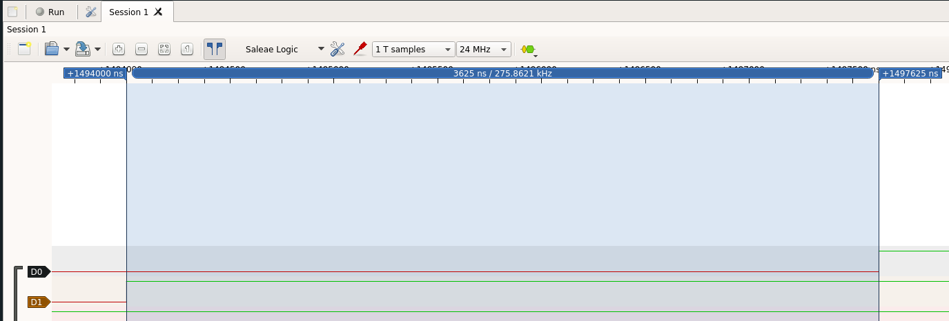
And indeed this can be measured using the logic analyzer, manual write delay is
125ns(8MHz) which is one instruction cycle. The digialWrite method has a delay
of 3625ns, which is a 29x increase. Including the 3 instructions for the
function parameter setup the 37 instruction delay is not reached, here I would
strongly guess that not all instructions have the same delay, maybe the 29x
comes from arithmetic instructions, instructions like cli might have a faster
timing, but yea not sure, although this can be measure, by placing instructions
between the two pin writes and measure the increase delay. This needs to done
via inline assembly.
Its also worth mentioning that setting the pins without the arduino library function decreases the program size by about 200 bytes.
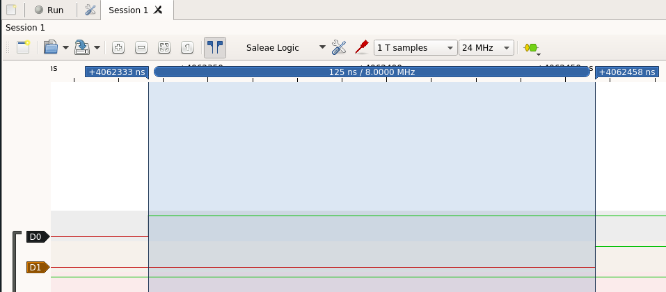
Adding a cli instruction via cli(); between the two pin sets, gives exactly one
extra instruction and the timing is indeed different, the delay is now 167ns,
the cli instruction adds 42ns. Lets test a view more instructions.
cli 42ns
clr 42ns
nop 42ns
eor 42ns
inc 42ns
mul 125ns

call 250ns
ret  250ns
call & ret  500ns
This shows some pretty nice timing differences.
Resources
- [1] https://github.com/nickgammon/arduino_sketches
- [2] https://circuitdigest.com/article/introduction-to-bit-banging-spi-communication-in-arduino-via-bit-banging
These two are especially nice
- http://www.gammon.com.au/forum/?id=11635
- http://www.gammon.com.au/forum/?id=11633
unsorted links
- https://docs.arduino.cc/built-in-examples/arduino-isp/ArduinoISP
- https://www.brainbytez.nl/hardware/arduino-burn-jtag-enabled-bootloader-on-arduino-mega-atmega2560/
- https://github.com/sowbug/JTAGWhisperer
- https://hsbp.org/fuji
- https://sourceforge.net/p/openocd/code/ci/master/tree/
- https://learn.adafruit.com/arduino-tips-tricks-and-techniques/bootloader